
|
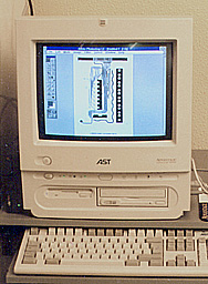
Step 1 Either use a CAD output to a laser printer or photocopy an image (from a magazine or template) onto the non-glossy side of a sheet of Press-n-Peel. The laser printed or photocopied circuit needs to be as dense as possible for best results. |
|
Step 2 Now you are ready to transfer the circuit to copper clad material which has been lightly scrubbed with scotchbrite or an abrasive to clean it. |
|
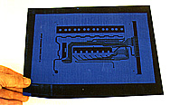
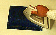
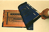
Step 3 Place the sheet face down on the copper clad material and iron it with an iron set halfway between two and three. Continue until the copper is hot and the image has gone dark all over. IT IS ESSENTIAL THAT YOU LET THE PRESS-N-PEEL AND THE COPPER CLAD MATERIAL COOL DOWN TO ROOM TEMPERATURE OR JUST ABOVE BEFORE YOU TRY TO PEEL IT. Otherwise some of the tracing may lift with the Press-n-Peel. |
|
Step 4 AFTER COOLING the film is peeled away to leave the image. If there are any nicks or bit missing then touch up with etch-resistant pen. Etching is by the normal method of Ferric or Clear Etchant in a tray or bubble etch tank. |
|
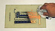
Step 5 AFTER ETCHING AND DRYING, remove the resist with PnP Stripper. The blue resist is stripped away leaving the copper circuit tracks. |
